
Analysis of mm-Wave CMOS Rectifiers and Ka-Band Implementation
Abstract
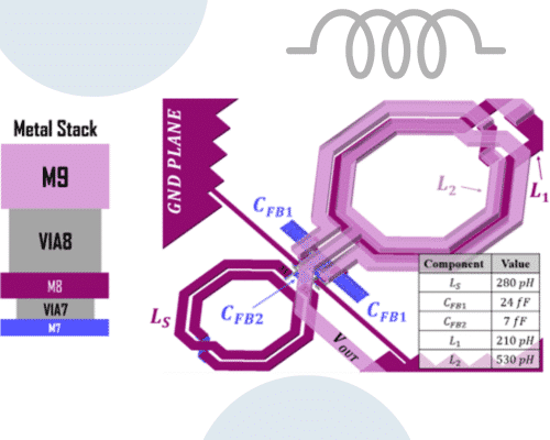
An in-depth millimeter-wave (mm-Wave) CMOS rectification analysis is presented, with an analysis methodology that enables a transient-based approach. The analysis sheds light on the mechanisms responsible for CMOS rectification and the limiting factors in the pursuit for higher power conversion efficiency (PCE). This article describes an innovative topology for 5G mm-Wave harvesting, using 65-nm CMOS. The rectifier circuit is based on a cross-coupled differential core that is enhanced by the addition of harmonic suppressing capacitors. Four versions of the topology are presented: two single rectifier circuits—with low voltage threshold (LVT) transistors and one with high voltage threshold (HVT) transistors; a voltage summing rectifier where two LVT rectifiers are placed in series; and a current summing rectifier where two LVT rectifiers are placed in parallel. The LVT and HVT single rectifiers achieve a peak PCE of 40% at 0-dBm input power and 42% at 7-dBm input power, respectively. Both series and parallel joining of two rectifiers yielded the same PCE as the single rectifier, with a higher current or voltage accordingly. Power offset measurements were carried out to emulate a real-world harvesting scenario of uneven power density across a rectenna array. All circuits are targeting the 5G new radio (NR) FR2 band between 26.5 and 29.5 GHz and present the state-of-the-art (SoA) results in a fully integratable solution.
https://ieeexplore.ieee.org/document/10016625