14:08 BST
 Silicon has been the mainstay of chips because silicon possesses a “Goldilocks” band gap of 1.1 electron Volts (eV), which makes it possible to operate integrated circuits at a low voltage, leading to reduced leakage of current. Another key feature of silicon is that it can be used to make a convenient “native” insulator, in the form of silicon oxide. Silicon oxide managed to serve as an insulator for silicon circuits for many generations of chips, isolating components and reducing gate leakage currents, until high-K dielectrics took over the job a decade ago.
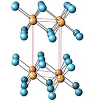
Now researchers at Stanford University and SLAC National Accelerator Laboratory have found that some of the most sought after high-K materials—namely hafnium selenide (HfSe2) and zirconium selenide (ZrSe2)—possess the same perfect band gap seen in silicon when they are thinned down to two-dimensional (2D) materials. As a result, the Stanford researchers have discovered a 2D material version of the handy silicon/silicon dioxide combination that enabled generations of chip designs. But in this case the combination can be shrunk down ten times smaller.