
An Ultrawideband Cryogenic LNA in 40-nm CMOS for Multiple Spin/Superconducting Qubit Readout
Abstract
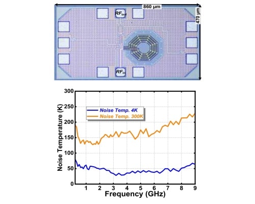
This letter presents an ultrawideband cryogenic low-noise amplifier (LNA) with current reuse and stacked inverter-based input-referred noise (IRN) cancellation in 40-nm CMOS. The first stage utilizes an IRN reduction high- Q gate inductor with current reuse, a stacked inverter-based shunt-resistive feedback input stage, and a cryogenically aware back-gate biasing technique to regulate the threshold voltage under cryogenic operation. The second stage is the common-source (CS) main amplifier, followed by a cascode current-reuse auxiliary amplifier to suppress the channel thermal noise of the main amplifier. The third stage is the current-reuse CS inverter-based postamplifier buffer stage. At 4 K, the LNA achieves a measured peak gain ( S21 ) of 37 dB, with a large 3-dB bandwidth (BW) from 0.15 to 8 GHz and a NFmin of 0.4 dB at 3.2 GHz under PDC of 13.2 mW. To our knowledge, the proposed LNA achieves the BW bandwidth and the figure of merit (FoM) among the highest compared to published CMOS LNAs operating at 4 K. The proposed LNA is suitable for both spin and superconducting qubit readout.
DOI: 10.1109/LMWT.2025.3631887 IEEEXplore:https://ieeexplore.ieee.org/document/11264819